logologo
  • HOME

  • PROGRAMS

  • PARTNERS

  • VISION

  • BLOG

  • CONTACT US

  • Home

  • About

  • Services

  • Courses

  • Contact Us
  • Home
  • Courses
  • Course Details

Physical Design

  • by Nidhi
  • English
  • (10 Rating)
About Nexsemi Academy

Nexsemi Academy offers cutting-edge digital solutions and research-driven
training across industries. Recognized as one of India's top technical training providers,
it specializes in RTL Design & Verification, Physical Design, Analog Layout, and more.
Known for unlimited placements, skill enhancement, and world-class training at affordable fees,
Nexsemi ensures students achieve excellent results and secure their first job from Day 1.
Our mission is simple: Equip every student with the best training and placement
opportunities to help them land their dream job.


  • shape
  • shape
  • shape

Course Description

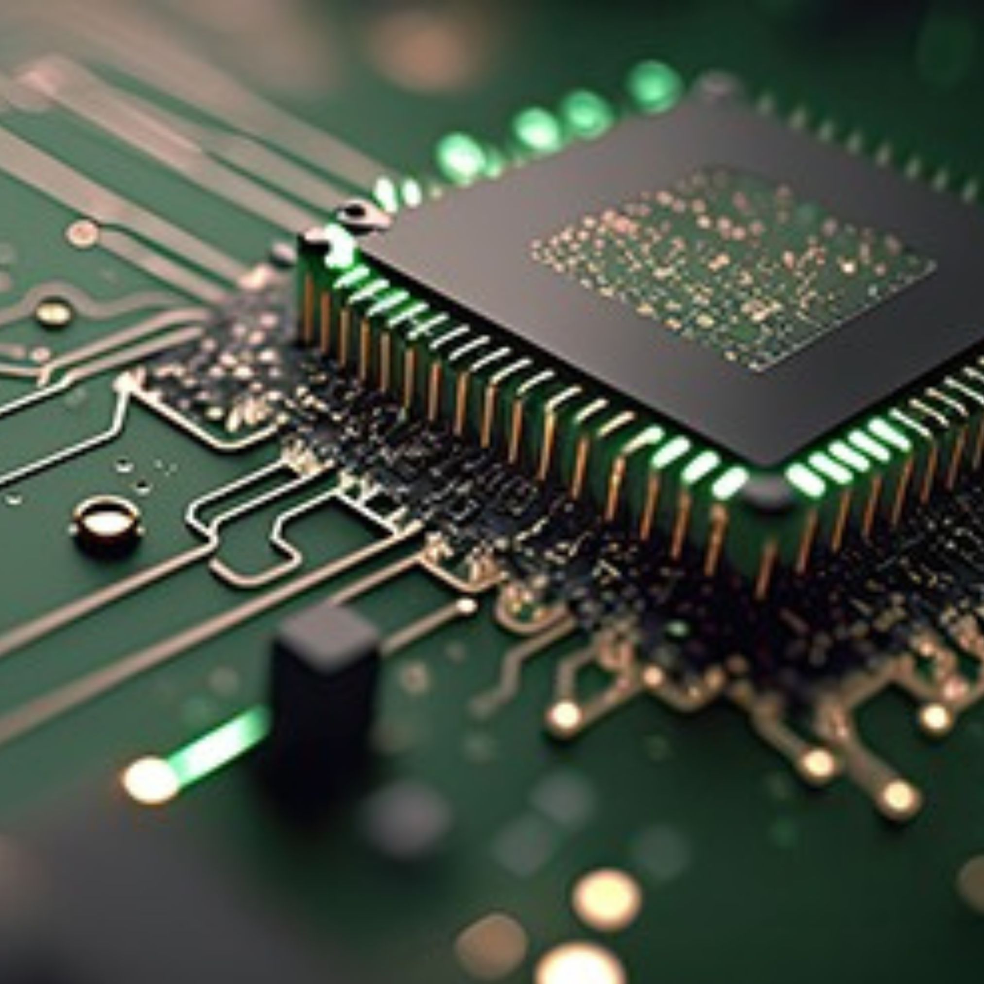
Physical design refers to the process of translating a high-level circuit description into a configuration that defines how an integrated circuit (IC) body used on a silicon wafer will operate. This phase includes activities such as placement, training, and optimization to ensure that the design meets all performance, power, and area requirements.

What You’ll Learn?
  • Floor Planning: Plan the important functions of the mold to optimize space and functionality.
  • Placement: Specify the location of modules or blocks on the floor plan.
  • Routing: Connecting components to the metal layer to create the desired circuit.
  • Optimization: Adjust the design to improve time, power, and area (PPA) metrics.

Physical design is a critical step in creating an efficient, robust, and reliable interface. Understanding physical design concepts, best practices, and tools can impact the success of your IC project. By keeping up with the latest trends and innovations, you can improve your design skills and meet the challenges of modern semiconductor manufacturing.We hope this guide will help you understand bodybuilding better. Subscribe to our blog and stay tuned for more tips and updates on IC design!


Course Curriculum

Lorem ipsum dolor sit amet, consectetur adipisicing elit, sed do eiusmod tempor inc idid unt ut labore et dolore magna aliqua enim ad minim veniam, quis nostrud exerec tation ullamco laboris nis aliquip commodo consequat.

Digital Design

  • Boolean Algebra
  • Logic Gates
  • Combinational logic design
  • Registers(SISO, SIPO, PISO, PIPO, USRM LFSR
  • Counters ( Asynchronous & Synchronous
  • FSM ( Melay and Moore - overlapping & Non overlapping
  • FIFO (Asynchronous, Synchronous)
Verilog

  • Data Types, Verilog Operators, Verilog verification and Assignments
  • Verilog Modelling Styles, System tasks
  • Design Methodologies - Top Down Bottom up
  • Adders, Latch, Flipflop, Counter, FSM, Shift registers
  • Logic Gates using MUX, Encoder, Decoder, Priority Encoder
  • Comparator, Seven Segment, Multipliers
  • Synthesizable vs Non-Synthesizable Constructs
  • Race Conditions in Verilog
CMOS Fundamentals

  • MOS Fundamentals
  • MOS IV Characteristics
  • CMOS Inverter Design
  • CMOS Design
  • Layout of inverter and NAND gate
  • Stick Diagrams
  • Stick Diagrams Eulers Method
  • Foundries: Semiconductors Eco System
  • Advancement in MOSFET
  • Introduction to CMOS
  • CMOS fundamentals
  • CMOS fabrication process
  • CMOS inverter
Synthesis

  • Introduction to Synthesis
  • Synthesis Flow
  • Constraining Design for timing, area & power Constraints development and understanding
  • Timing Library (.lib) formats
  • Design Timing Checks
  • Analyze and debug results
  • Optimization Techniques
  • DFT basics
Inputs Files & Sanity Check

  • List of inputs
  • Libraries, technology files, netlist, timing constraints, IO placement
  • Understanding input file
  • Qualifying the received inputs and sanity checks
  • Low power implementation techniques
Floorplaning Concepts and IO Placement

  • Why and what is floor planning?
  • Different parameters of floor planning
  • Floor planning guidelines
  • Square/Rectangle/Rectilinear Floorplans
  • Macro placement
  • IO placement
  • Channel-width estimation
Placement

  • Why and what is Placement ?
  • Types of placements ?
  • Pre-place optimization and in-place optimization
  • Pre-place (End-cap, Tap & I/O Buffer) cells
  • Congestion analysis, timing analysis
  • High-Fanout Net Synthesis
  • Tie-cells
  • Scan chain re-
  • Regioning/Grouping/Bounds
Timing Analysis & Optimization

  • Setup-hold & timing checks
  • Understanding timing constraints(SDC)
  • Corners timing
  • Timing report analysis
  • Optimization techniques
  • Cause for timing violations and strategies for fixing
Clock Tree Synthesis (CTS)

  • Clock Tree Structure
  • Clock Latency
  • Clock Buffer & Inverter
  • Clock Gating
  • CDC
Routing design and optimization

  • Why Routing is required ?
  • Different Types-of Routing
  • Fix routing violations (DRC, LVS)
  • Post routing optimization
  • Issues in routing and guide lines for optimum routing results
ECO Flow

  • What is ECO? Types of ECO Timing & Functional ECO prep Performing the ECO
  • Placement and Routing
Sign-off Checks

  • Design Rule Checks understanding and importance
  • Layout Versus Schematic and difference with respect to LEC
  • Electrical Rule Check
  • Electro-Migration Analysis
  • IR drop analysis
  • Cross-Talk (SI) analysis
  • Sign-off Timing analysis
  • Logical Equivalence checking
TCL Scripting and Perl Scripting

  • TCL and Perl commands
  • Variables Expressions
  • Identifiers Comments
  • Reserved words Data
  • Types Arrays and strings
  • Loops I/O Files


team images
Nidhi
Founder & CEO

Consectetur adipisicing elit, sed do eiusmod tempor incididunt labore et dolore magna aliqua enim minim veniam quis nostrud exercitation ulla mco laboris nisi ut aliquip ex ea commodo consequat. duis aute irure dolor in reprehenderit in voluptate.


Course Rating

4.4 average rating based on 10 rating

4.4
(10 Review)
5
10
5
0
5
0
5
0
5
0

Reviews

Comment Images
Oct 10, 2021

Lorem ipsum dolor sit amet, consectetur adipisicing elit sed do eiusmod tempor incididunt ut labore et dolore magna aliqua.

Comment Images
Oct 15, 2021

Lorem ipsum dolor sit amet, consectetur adipisicing elit sed do eiusmod tempor incididunt ut labore et dolore magna aliqua.

Comment Images
Oct 19, 2021

Lorem ipsum dolor sit amet, consectetur adipisicing elit sed do eiusmod tempor incididunt ut labore et dolore magna aliqua.

Write a Review

Rating Here
Course Thumb

Course Includes:

  • Price:Rs.10000-70000
  • Instructor:Nidhi
  • Duration:300 Hours
  • Lessons:8
  • Enrolled: students
  • Language:English
  • Certificate:yes

Share On:

Corporate Logo

  • Add:4th Floor, No 14, K No 25/2, Hobli, Chinnappanahalli, Anand Nagar, K.R. Puram, Chinnapanna Halli, Bengaluru, Karnataka 560037
  • Call:9740545514
  • Email:NexsemiAcademy@gmail.com

Links

  • About
  • Courses
  • PARTNERS

Links

  • Contact Us
  • Events
  • VISION
  • BLOG

Contacts

Enter your email address to register to our newsletter subscription

Copyright 2025 Nexsemi Designed By Strix Digital. All Rights Reserved